Our YouTube channel: @implantMD
YOUTUBE @implantMDTutorials for compilation of scientific software and supplementary videos showcasing our work.
See our expertise portfolio:
Surface modification
Ion implantation
Contact person: Ing. Petr Vlčák, PhD → petr.vlcak@fs.cvut.cz
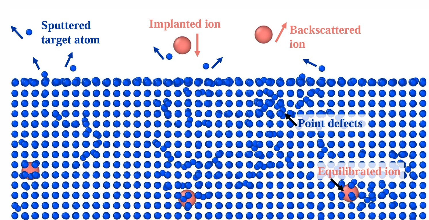
We perform experiments involving ion implantation of nitrogen, oxygen, and argon to study their impact on the materials surface properties. Ion implantation utilizes bombardment of a target material with ion particles (dopants) to modify its properties, such as electrical and thermal conductivity, corrosion resistance, wettability, wear resistance, hardness, or biocompatibility. The majority of the implanted ions (at perpendicular incidence) penetrate below the target surface and attain equilibrium state, while a minor fraction is backscattered. Additionally, some target atoms are sputtered from the surface. The resulting alterations in material properties can be adjusted by varying implantation parameters, such as ion fluence (the number of ions impacting the target per unit area during the total implantation time), ion type, ion energy, ion incidence angle, target state and composition, target temperature, and target crystallographic orientation.
Thin film deposition
Physical vapor deposition
Contact person: doc. Ing. Petr Vlčák, Ph.D. → petr.vlcak@fs.cvut.cz
We utilize physical vapor deposition (PVD) technique to deposit thin film layers onto a substrate. The PVD process involves the vaporization of a target material via sputtering, wherein high-energy argon ions bombard the target, causing the ejection of its atoms. These vaporized atoms subsequently condense on the substrate surface, leading to the formation of a thin film. The PVD process is performed in a vacuum chamber to minimize contamination. This technique allows us to deposit various materials, including metals, ceramics, or polymers.

Material modeling
Computer simulations
Contact person:
Ing. Jan Drahokoupil, Ph.D. → draho@fzu.cz
Ing. Miroslav Lebeda → lebedmi2@cvut.cz
We conduct Monte Carlo (MC, in TRIM and TRIDYN), molecular dynamics (MD, in LAMMPS), and density functional theory (DFT, in VASP and Quantum ESPRESSO) simulations to investigate changes in materials properties connected with the ion implantation and to improve the interpreation of experimental data. In general, MC uses pseudo-random numbers and probability distributions to statistically analyze behavior of the studied system. TRIM and TRIDYN are specific MC software based on binary collision approximation (BCA) for predicting the ion implantation results. MD is a deterministic numerical method for simulating the interactions and trajectories of atoms. The atoms are approximated as point objects and interatomic forces are calculated from a pre-defined potential field. Newton’s second law is used to integrate atomic equations of motion and determine positions and velocities at the following timestep. Because MD is capable of computations with tenths of thousands of atoms, it can directly simulate the processes of ion implantation or nanoindentation. DFT is a quantum mechanical approach to compute the electronic structure of the matter. It is based on the principle of finding the ground state electron density (rather than the wavefunction itself) by varying and minimizing the total system energy functional. It predics properties such as ground state energies, adsorption energies, defects energies, surface energies, electron band-structures, phonon spectra, lattice parameters, elastic coefficients, elastic moduli, and various spectra including infrared, Raman, and EELS.
Material characterization
X-rays techniques
Contact person: Ing. Jan Drahokoupil, Ph.D. → draho@fzu.cz
We employ X-ray based techniques such as X-ray diffraction (XRD), small angle X-ray scattering (SAXS, GISAXS), and micro computed tomography (micro-CT) to characterize materials crystal structure, microstructure, and texture. XRD entails the examination of a diffraction pattern that arises from the constructive interference of scattered X-rays, which is caused by the periodic ordering of atoms in a crystal lattice. Intensities, angles at which the diffracted beams are observed (Bragg angles), and peak widths carry a footprint on the structural and microstructural information of the material. The major XRD applications include qualitative and quantitative phase analysis, estimation of crystallite sizes, evaluation of residual stresses, and determination of lattice parameters. SAXS utilizes detection of X-rays scattered at low angles to investigate the microscture and nanosctructure of materials. It is commonly used to determine the size and shape distribution of nanoparticles, macromolecules, or pores. Micro-CT is a non-destructive imaging technique used to create high-resolution 3D images of the internal microstructure of materials, allowing to analyze features with micro dimensions, such as pores, inclusions, and cracks.

Material characterization
Corrosion testing
Contact person: Ing. Šimon Svoboda → simon.svoboda@fs.cvut.cz
We carry out electrochemical corrosion testing to assess the corrosion resistance of metallic materials and thin-film coatings. Potentiodynamic polarization measurements in Hank’s solution are used to determine corrosion potential, corrosion current density, and passivation behavior, providing insight into coating stability in simulated physiological environments.

Material characterization
Atomic force microscopy
Contact person: Ing. Vojtěch Smola → vojtech.smola@fs.cvut.cz
We use atomic force microscopy (AFM) to obtain a topographical image of a sample surface with the nanoscopic resolution, as well as a variety of mechanical, functional, and electrical properties. AFM employs a sharp probe tip attached to a cantilever which scans the sample’s surface. During scanning, the forces between the tip and the atoms are analyzed and processed to generate the topographical image. Unlike scanning tunneling microscopy, AFM does not require a conducting sample.

See our previous project:
